- 您现在的位置:买卖IC网 > Sheet目录2000 > IDTCV110NPVG (IDT, Integrated Device Technology Inc)IC FLEXPC CLK PROGR P4 56-SSOP
COMMERCIALTEMPERATURERANGE
2
IDTCV110N
PROGRAMMABLEFLEXPCCLOCKFORP4PROCESSOR
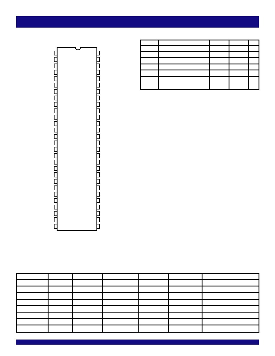
PIN CONFIGURATION
Symbol
Description
Min
Max
Unit
VDDA
3.3V Core Supply Voltage
4.6
V
VDD
3.3V Logic Input Supply Voltage GND - 0.5
4.6
V
TSTG
Storage Temperature
–65
+150
° C
TAMBIENT
Ambient Operating Temperature
0
+70
° C
TCASE
Case Temperature
+115
° C
ESD Prot
Input ESD Protection
2000
V
Human Body Model
ABSOLUTE MAXIMUM RATINGS(1)
NOTE:
1. Stresses greater than those listed under ABSOLUTE MAXIMUM RATINGS may cause
permanent damage to the device. This is a stress rating only and functional operation
of the device at these or any other conditions above those indicated in the operational
sections of this specification is not implied. Exposure to absolute maximum rating
conditions for extended periods may affect reliability.
SSOP
TOP VIEW
56
55
54
53
52
51
50
49
48
47
46
45
44
43
42
41
40
39
38
37
36
35
34
33
32
31
30
29
PCI2
PCI1
PCI0
FSC/TEST_SEL
REF
VSS_REF
XTAL_IN
XTAL_OUT
VDD_REF
SDA
SCL
VSS_CPU
CPU0
CPU0#
VDD_CPU
CPU1
CPU1#
IREF
VSSA
VDDA
CPU2_ITP/SRC7
CPU2_ITP#/SRC7#
VDD_SRC
SRC6#
SRC5
SRC5#
VSS_SRC
1
2
3
4
5
6
7
8
9
10
11
12
13
14
15
16
17
18
19
20
21
22
23
24
25
26
27
28
VDD_PCI
VSS_PCI
PCI3
PCI4
PCI5
VSS_PCI
VDD_PCI
PCIF0/ITP_EN
PCIF1
VTT_PWRGD#/PD
VDD48
USB48
VSS48
DOT96
DOT96#
FSB/TEST_MODE
PCIF2
FSA
SRC1
SRC1#
VDD_SRC
SRC2
SRC2#
SRC3
SRC3#
SRC4
SRC4#
VDD_SRC
SRC6
FREQUENCY SELECTION TABLE
FSC, B, A
CPU
SRC[7:1]
PCI
USB
DOT
REF
101
100
33.3
48
96
14.318
001
133
100
33.3
48
96
14.318
011
166
100
33.3
48
96
14.318
010
200
100
33.3
48
96
14.318
000
266
100
33.3
48
96
14.318
100
333
100
33.3
48
96
14.318
110
400
100
33.3
48
96
14.318
111
Reserve
100
33.3
48
96
14.318
发布紧急采购,3分钟左右您将得到回复。
相关PDF资料
IDTCV115-2PVG
IC FLEXPC CLK PROGR P4 56-TSSOP
IDTCV115FPVG
IC FLEXPC CLK PROGR P4 56-SSOP
IDTCV119EPVG8
IC CLK GEN DESKTOP PC 48-SSOP
IDTCV133PAG
IC FLEXPC CLK PROGR P4 56-TSSOP
IDTCV136PAG
IC FLEXPC CLK ATI RS400 56-TSSOP
IDTCV137PAG
IC FLEXPC CLK AMD K8 56-TSSOP
IDTCV142PAG
IC FLEXPC CLK PROGR P4 56-TSSOP
IDTCV146PVG
IC FLEXPC CLK PROGR P4 56-SSOP
相关代理商/技术参数
IDTCV110NPVG8
功能描述:IC FLEXPC CLK PROGR P4 56-SSOP RoHS:是 类别:集成电路 (IC) >> 时钟/计时 - 专用 系列:FlexPC™ 标准包装:28 系列:- 类型:时钟/频率发生器 PLL:是 主要目的:Intel CPU 服务器 输入:时钟 输出:LVCMOS 电路数:1 比率 - 输入:输出:3:22 差分 - 输入:输出:无/是 频率 - 最大:400MHz 电源电压:3.135 V ~ 3.465 V 工作温度:0°C ~ 85°C 安装类型:表面贴装 封装/外壳:64-TFSOP (0.240",6.10mm 宽) 供应商设备封装:64-TSSOP 包装:管件
IDTCV111IPAG
制造商:Integrated Device Technology Inc 功能描述:400 MHz, PROC SPECIFIC CLOCK GENERATOR, PDSO56
IDTCV115-2
制造商:IDT 制造商全称:Integrated Device Technology 功能描述:PROGRAMMABLE FLEXPC? CLOCK FOR P4 PROCESSOR
IDTCV115-2PV
功能描述:IC FLEXPC CLK PROGR P4 56-TSSOP RoHS:否 类别:集成电路 (IC) >> 时钟/计时 - 专用 系列:FlexPC™ 标准包装:1,500 系列:- 类型:时钟缓冲器/驱动器 PLL:是 主要目的:- 输入:- 输出:- 电路数:- 比率 - 输入:输出:- 差分 - 输入:输出:- 频率 - 最大:- 电源电压:3.3V 工作温度:0°C ~ 70°C 安装类型:表面贴装 封装/外壳:28-SSOP(0.209",5.30mm 宽) 供应商设备封装:28-SSOP 包装:带卷 (TR) 其它名称:93786AFT
IDTCV115-2PV8
功能描述:IC FLEXPC CLK PROGR P4 56-TSSOP RoHS:否 类别:集成电路 (IC) >> 时钟/计时 - 专用 系列:FlexPC™ 标准包装:1,500 系列:- 类型:时钟缓冲器/驱动器 PLL:是 主要目的:- 输入:- 输出:- 电路数:- 比率 - 输入:输出:- 差分 - 输入:输出:- 频率 - 最大:- 电源电压:3.3V 工作温度:0°C ~ 70°C 安装类型:表面贴装 封装/外壳:28-SSOP(0.209",5.30mm 宽) 供应商设备封装:28-SSOP 包装:带卷 (TR) 其它名称:93786AFT
IDTCV115-2PVG
功能描述:IC FLEXPC CLK PROGR P4 56-TSSOP RoHS:是 类别:集成电路 (IC) >> 时钟/计时 - 专用 系列:FlexPC™ 标准包装:1,500 系列:- 类型:时钟缓冲器/驱动器 PLL:是 主要目的:- 输入:- 输出:- 电路数:- 比率 - 输入:输出:- 差分 - 输入:输出:- 频率 - 最大:- 电源电压:3.3V 工作温度:0°C ~ 70°C 安装类型:表面贴装 封装/外壳:28-SSOP(0.209",5.30mm 宽) 供应商设备封装:28-SSOP 包装:带卷 (TR) 其它名称:93786AFT
IDTCV115-2PVG8
功能描述:IC FLEXPC CLK PROGR P4 56-TSSOP RoHS:是 类别:集成电路 (IC) >> 时钟/计时 - 专用 系列:FlexPC™ 标准包装:28 系列:- 类型:时钟/频率发生器 PLL:是 主要目的:Intel CPU 服务器 输入:时钟 输出:LVCMOS 电路数:1 比率 - 输入:输出:3:22 差分 - 输入:输出:无/是 频率 - 最大:400MHz 电源电压:3.135 V ~ 3.465 V 工作温度:0°C ~ 85°C 安装类型:表面贴装 封装/外壳:64-TFSOP (0.240",6.10mm 宽) 供应商设备封装:64-TSSOP 包装:管件
IDTCV115-4PVG
功能描述:IC FLEXPC CLK PROGR P4 56-SSOP RoHS:是 类别:集成电路 (IC) >> 时钟/计时 - 专用 系列:FlexPC™ 标准包装:1,500 系列:- 类型:时钟缓冲器/驱动器 PLL:是 主要目的:- 输入:- 输出:- 电路数:- 比率 - 输入:输出:- 差分 - 输入:输出:- 频率 - 最大:- 电源电压:3.3V 工作温度:0°C ~ 70°C 安装类型:表面贴装 封装/外壳:28-SSOP(0.209",5.30mm 宽) 供应商设备封装:28-SSOP 包装:带卷 (TR) 其它名称:93786AFT